Transition metal dichalcogenide monolayers
Recently, we have outlined new concepts that enable an exciting class of materials, which we have coined “dynamically programmable electromechanical 2D materials”. This class of materials is comprised of 2D monolayers capable of rapid, mechanically-induced local phase transitions at the nanoscale and above between crystalline domains with qualitatively different charge transport properties. This feature can be used to dynamically “draw” localized, strain-induced conducting regions in an otherwise semiconducting transition metal dichalcogenide (TMD) monolayer. We propose that this concept can be exploited to create interesting new micro- and nanoelectromechanical devices (MEMS and NEMS).
While existing strain engineering and phase engineering approaches can already enable extraordinary tailoring of optoelectronic properties in 2D materials, they are typically applied either reversibly via strain homogeneously throughout the monolayer or irreversibly via, e.g., laser irradiation in localized regions. Recent work has led to the proposal of simultaneous strain/phase engineering for phase control via strain-induced crystal structure transformations in Group VI TMD monolayers. We believe that this concept has tremendous potential as a means of enabling localized dynamic/reversible phase control at the nanoscale and above, which in turn opens a number of interesting device-relevant functionalities. Knowledge gaps that we believe must be addressed to realize this potential include: 1) understanding how such transformations occur in terms of domain physics, microstructural evolution, monolayer bending effects, etc., 2) mapping of strain phase diagrams for various TMD systems, 3) discovery of specific means of dynamic/on-the-fly strain-programming, and 4) extension and translation of the concept to specific MEMS/NEMS device applications. Each of these issues has been addressed in recent work from our group.
To this end, we have introduced a new, broadly applicable multi-scale modeling tool that quantitatively describes structural transformations in bendable 2D TMD monolayers by coupling first-principles computations with a mesoscale continuum approach. Using this method, we have characterized general features of domain evolution in the semiconducting (H) to metallic/semi-metallic (T’) transformation in Group VI TMDs, using MoTe2 and WTe2 as representative systems. We have also explored several strategies for how to spatially modulate strain to produce patterns of semiconducting and metallic regions within a single TMD layer through application of localized mechanical loads and/or patterning of substrates. A variety of extensions of these concepts, that allow practical exploitation for interesting devices, were also identified. For example, strains can be used to “rewire” a device on demand, to create MEMS/NEMS with no moving parts, or to strategically modify localized charge/spin transport behavior of origami and kirigami-based material designs.
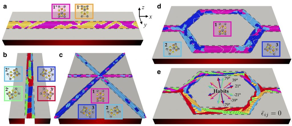
The figure at the top displays simulated buckling-facilitated T’ patterning in WTe2 in a channel geometry. Grey regions are bound to the substrate to produce a predominantly H layer. Regions between the dashed lines are suspended over channels in the substrate. The suspended regions buckle and transform to T’, and the variant selection is dictated by applied strain and channel orientation. In the animation below, inhomogeneous strain from the application of two indenters results in the formation of a conducting T’ domain between the two indenter tips.
More information can be found in the following articles: J. Berry et al., Nano Letters (2017), J. Berry et al., Phys. Rev. Materials (2018), and Xia et al., Nano Letters (2019).
